
| How to Measure Nanometers: Capacitive Sensors / for Nano-Measuring / Nanometrology | |||
 | Capacitive sensors (capacitance gauges) are the nanometrology technology of choice for the most demanding precision positioning, scanning and measurement applications, when it comes to measuring small distances with nanometer resolution and below. PI capacitive sensors ensure highest accuracy, resolution, linearity and long-term stability. These absolute-measuring, non-contact devices detect motion
at sub-nanometer levels without contact, directly. They provide a combination of accuracy, linearity, resolution, stability and bandwidth superior to conventional sensors such as LVDTs and strain gauge type sensors (piezo resistive sensors). Capacitive sensors are used in 6-axis nanopositioning metrology stages. For long travel motion systems such as 6-axis Hexapod robots, encoder type sensors are used.
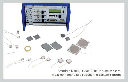
For the ultimate performance the D-015 - D-100 two plate sensor series are available. The single-probe D-510 series provide similar precision and feature an integrated LEMO connector for easy mounting and replacement in the field.
|
 Tutorial: Capacitive Position Sensors Measuring with Sub-nanometer Precision
Read on or jump to the Capacitance Sensor Selection Guide
Download the Capacitive Sensors Brochure
Tutorial: Capacitive Position Sensors Measuring with Sub-nanometer Precision
Read on or jump to the Capacitance Sensor Selection Guide
Download the Capacitive Sensors Brochure | ||
| Applications for Capacitive Position Sensors | ||||||||
| Click on the images for more information | ||||||||
 |
 |
 |
 |
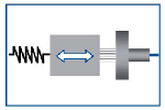 | ||||
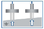
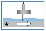
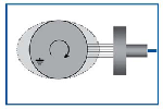
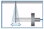
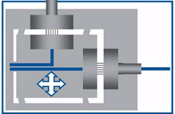
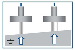
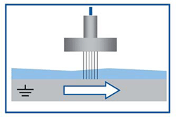
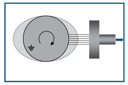
| Measuring Displacement with Nanometer Precision | Nanopositioning / Closed-Loop Systems | Parallel Metrology / High-Precision Multi-Axis Measurements | Measuring Straightness and Flatness / Active Cross-Talk Compensation | Force Sensors with Micronewton Sensitivity | ||||
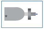
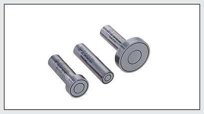
| Single-Probe Capacitive Position Gauge for Nanometrology Applications | ||
| The D-510 family of PISeca™ single-electrode capacitive displacement gauges performs high-precision, non-contact measurements of geometric quantities representing displacement, separation, position, length or other linear dimension against any kind of electrically conductive target. These single-probe nanometrology sensors combine superior resolution and linearity with very high bandwidth for dynamic measurements. | ||
 D-510 Single-Probe Capacitive
Position Gauge for Nanometrology Applications | Features & Advantages
| |
|
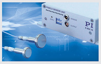
Higher Linearity through Guard-Ring Capacitor and ILS Electronics Not all capacitive sensors are created equal. Because the sensor design has a strong influence on the linearity, PI uses a special guard-ring electrode to shield the sensor electrode from boundary effects. This ensures a homogeneous electric field in the measurement zone and results in higher measuring linearity. In addition, the E-852 sensor signal conditioning electronics are equipped with the PI proprietary ILS linearization circuit. Easy Installation & Setup The capacitive gauges are plug and play units. A high cable with a performance LEMO connector plugs directly into the sensor head for easy installation or replacement in the field. Installation is further facilitated by a display in the E-852 signal conditioner sensor electronics that indicates the optimum distance between probe and target. | ||
|
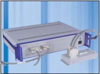
E-852 Signal Conditioner Electronics for D-510 | ||
|
E-509.E03 E-509.E3 3-Channel Electronics for D-510 PISeca Sensors | ||
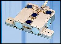
| Direct Metrology, Parallel Metrology Configurations |
| The capacitance sensors offered by PI are the most accurate measuring systems for nanopositioning applications currently on the market. In contrast to high-resolution sensors measuring deformation in the drive train, like strain gauge or piezoresistive sensors, capacitive sensors are non-contact, direct-metrology devices—a fact which gives them many advantages: |
|
|
 Capacitive position sensors in an ultra-high-accuracy,
 | Capacitive sensors are especially well-suited for parallel metrology configurations. In multi-axis nanopositioning systems, parallel metrology means that the controller monitors all controlled degrees of freedom relative to "ground" (the fixed frame) and uses each actuator to compensate the undesired off-axis motion of the others automatically (active trajectory control). As a result, it is possible to keep deviations in the sub-nanometer and sub-microradian range. |
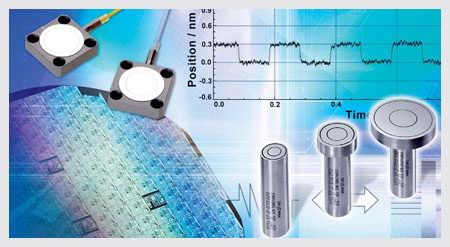
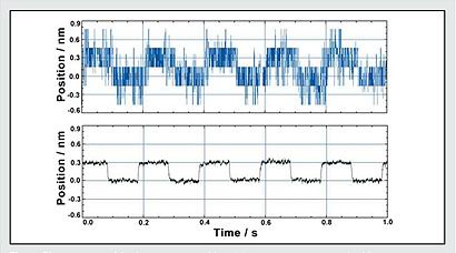
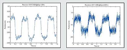
Figure 1 shows a D-015, 15 m capacitive position sensor and an interferometer,
both measuring nanometer-range actuator cycles. The graphs clearly show the superior resolution of the capacitive position sensing technique. 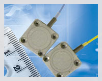
D-050 Capacitance Sensor Probes. |
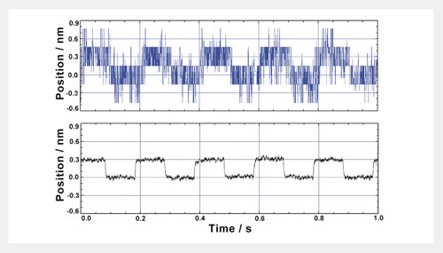 Fig 1. Piezo nanopositioning system making 0.3 nm steps, measured with PI capacitive sensor (lower curve) and with a laser interferometer. The capacitive sensor can provide even higher resolution than the interferometer | |
| Read on or jump to the Capacitance Sensor Selection Guide |
| Stability and Linearity of PI Capacitive Position Sensors |
| PI capacitive position sensor electronics incorporate a proprietary design providing
superior linearity, low sensitivity to cable capacitance, low background noise and low drift.
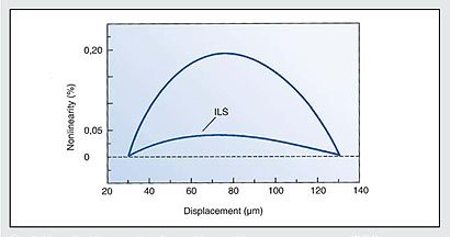
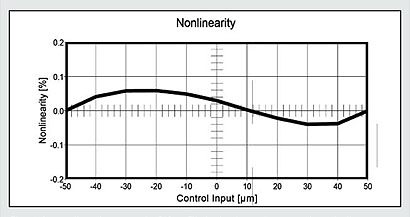
The Integrated Linearization System (ILS) compensates for influences caused by errors, such as non-parallelism of the plates. When used with PI digital controllers (which add polynomial linearization techniques) a positioning linearity of up to 0.003 % is achievable. Figure 2 shows the linearity of a P-752.11C piezo flexure nanopositioning stage with integrated capacitive position sensor operated in closed-loop mode with an analog controller. All errors contributed by the mechanics, PZT drive, sensors and electronics are included in the resulting linearity of better than 0.02 %. Even higher linearity is achievable with PI digital controllers. The exceptional long-term stability of the PI capacitive position sensor and electronics design is shown in Figure 3. |
| Fig 2. Linearity of a P-752.11C, 15 m piezo nanopositioning stage operated with E-500/E-509.C1 control electronics. The travel range is 15 m, the gain 1.5 m/V. Linearity is better than 0.02 %; even higher linearity is achievable with PI digital controllers |
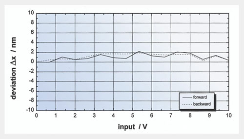 Fig. 2 | |
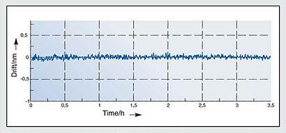
| Fig 3. Measurement stability of an E-509.C1 capacitive position sensor control board with 10 pF reference capacitor over 3.5 hours (after controller warm-up). | 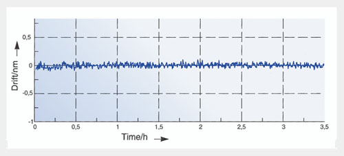 Fig. 3 | |
| Read on or jump to the Capacitance Sensor Selection Guide | ||
|
E-852 Signal Conditioner Electronics for D-510 |
| Special Design Eliminates Cable Influences |
 |
When measuring distance by detection of capacitance changes, fluctuations in the cable capacitance can
have an adverse effect on accuracy. This is why most capacitive measurement systems only provide satisfactory results with short, well-defined cable lengths.
PI Systems use a special design which eliminates cable influences, permitting use of cable lengths of up to 3 m without difficulty. For optimum results, we recommend calibration of the sensor-actuator system in the PI Metrology Lab. Signal Paths to 15 Meters and More Longer distances between sensor and electronics can be spanned with special, loss-free, digital transmission protocols. A remote sensor interface box is available for PI digital controllers . |
| Features & Advantages, Applications | ||
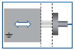
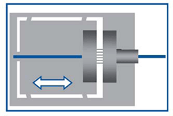
 Two-plate capacitive sensor working principle.  Quality control and long-term stability testing of capacitive displacement sensors at PI.  Custom, 7-channel, capacitive position sensor electronics.
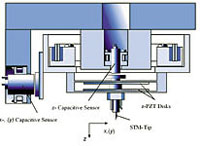 Working principle of STM (scanning tunneling microscope) with
integrated capacitive position sensors
Working principle of STM (scanning tunneling microscope) with
integrated capacitive position sensors |
Properties of PI Sensors
Reasons for Choosing PI
 | |
|
Capacitive Sensors Catalog | ||
| Tutorial: Capacitive Position Sensors Measuring Displacement with Sub-Nanometer Precision | |||
| Glossary | |||||
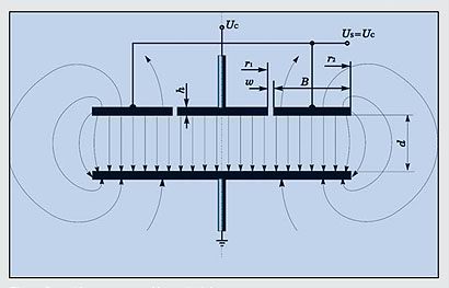
| Measurement Range | |||||
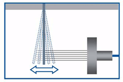
| The measurement range depends on the size of the active sensor area as well as on the electronics used.
Due to PIs proprietary signal conditioner electronics design,the mid-range distance is always identical to the selected measurement range. The probe-to-target gap may vary from 50% to 150% of the measurement range (see Fig. 14). The sensor capacitance is the same as that of the reference capacitance in the electronics. Different reference capacitance scan be used to extend the nominal (standard) measurement range (see Fig. 15). | 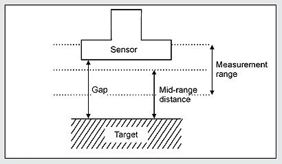 Fig. 14: Definitions: measurement range and mid-range distance have identical values | ||||
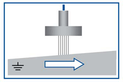
| Target | |||||
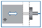
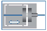
| Two-electrode capacitive sensors consist of two electrodes, named probe and target. Single-electrode sensors measure against a surface that is called the target.
The target surface is, in principle, a conductive material electrically connected to ground. Measurement against semiconductors is possible as well. While two-plate capacitive sensors consist of two well-defined high-quality planes, with single-plate sensors, target surface characteristics can influence the results. A curved or rough surface will deteriorate the resolution because the results refer to an average gap (see Fig. 16 and 17). Surface shape also influences the homogeneity of the electric field and thereby the measurement linearity. For factory calibration, a target plane that is considerably larger than the sensor area is used. | 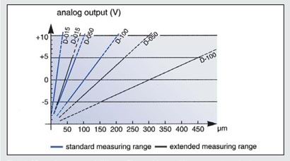 Fig. 15: Measuring ranges of different PI capacitive position sensors (standard ranges in blue, extended ranges in black) | ||||
| Environment | |||||
| Precision measurement with nanometer accuracy requires minimizing environmental influences. Constancy of temperature and humidity during the measurement are as essential as cleanliness.
Electronics from PI are basically very temperature stable. Temperature drift is under 0.2% of full measurement range with a change of temperature of 10 C. Temperature changes also cause all material in the system to expand or contract, thus changing the actual measured gap. The influence of a change in relative humidity of 30 percentage points is less than 0.5% of the measurement range. Condensation must always be avoided. Dusty or damaged sensor surfaces will also worsen the measurement quality. Environmental conditions at the time of calibration are noted on the calibration sheet PI provides with each individual system. |  Fig. 16: Roughness of the target surface downgrades resolution and linearity 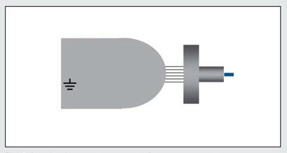 Fig. 17: Curved surfaces lead to an averaged distance measurement Fig. 17: Curved surfaces lead to an averaged distance measurement | ||||
| PI Solutions for Nano-Measuring / Positioning | ||
| Introduction | ||
|  | |
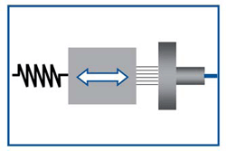
| One- and Two-Plate Sensors
Capacitive sensors perform non-contact measurements of geometric quantities representing distance, displacement, separation, position, length or other linear dimensions with sub-nanometer accuracy. PI offers capacitive sensors for the inte-gration in user applications in two-plate-capacitor versions for highest performance and asPISeca single-electrode sensors, for more flexibility and easier integration.
Nanopositioning and Nanometrology
Measurement Principle
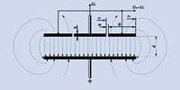
| conductive surfaces set up a homogenous electric field; for short distances, the applied voltage is proportional to the distance between the plates. Dual-plate sensors measure the distance between two well-defined sensor plates with carefully aligned surfaces which generate the most accurate electric field and hence provide optimal results. Single-plate capacitive sensors measure the capacitance against electrically conductive references, such as metallic plates, and are very convenient to install and connect.
Test and Calibration
PI calibrates every capacitive measurement system individually, optimizing the performance for the customers application. Such precision is the basis of all PI products, standard and customized, and assures optimum results in the most varied of applications. | |
| Function, Properties, Advantages | ||
| Introduction | ||
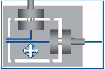
| In the field of nanopositioning, as well as for scanning and metrology applications, capacitive measurement systems from PI provide highest accuracy available at various measurement ranges. Capacitive sensors achieve the best possible measurement linearity and excellent long-term stability. The sensors provide contact-free measurement of the actual position of the moving part (direct metrology) with sub-nanometer precision. Accuracy, linearity, resolution, stability and bandwidth are far better than with conventional nano-metrology sensors like LVDT or strain gauge sensors. Non-contact operation means no parasitic forces influencing the application and results in measurement free of friction and hysteresis. Guard-Ring Design for Improved Linearity Sensor design has a strong influence on linearity. The superior PI design uses a guard-ring electrode that eliminates sensor electrode boundary effects. This ensures a homogenous field in the measurement zone and results in higher measuring linearity. Single- and Multi-Channel Electronics PIs signal conditioner electronics are specially designed for high bandwidth, linearity and ultra-low noise and are perfectly matched to the various PI sensor probes. PI offers signal conditioner electronics and controllers for one to three channels. The E-509 multichannel modules plug into the modular E-500 / E-501 controller chassis. Bandwidth and measurement range can be factory- set to meet the specific needs of each application. The E-852 one-channel signal conditioner electronics for PISeca single-plate sensors are designed as stand-alone systems with user-selectable bandwidth and range setting and can be synchronized to operate in multi-channel applications. Higher Linearity through ILS Electronics All of PIs signal conditioning electronics are equipped with the PI proprietary ILS linearization circuit that minimizes nonparallelism errors. Easy Handling and Integration PISeca single-electrode sensors are particularly easy to install in a measurement system. On the single-channel electronics, an LED-bar indicates the optimum probe-to-target gap for the different measurement range settings. The multi-channel electronics come optionally with displays and/or a PC interface on a module in the same housing. Ideal for Closed-Loop Piezo Nanopositioning Closed-loop nanopositioning systems may be controlled by sensor / servo-controller modules of PIs E-500 series. Such modules are available for connecting up to three position sensors, either stand-alone or integrated into the motion system. Closed-loop operation eliminates the drift and hysteresis that otherwise affect piezo actuators. For nanopositioning tasks with the most stringent accuracy requirements PI offers high end digital controllers. | 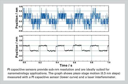 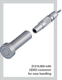 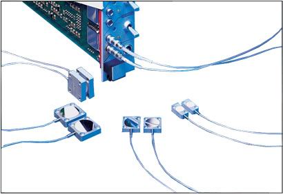 Capacitive 2-plate sensors from PI, here D-100.00 | |
| Capacitance Sensor Selection Guide |
|
| |||||
Single and Dual Probe Nanometrology Position Sensors | |||||
| Models* | Description | Measurement Range [m] Nominal / Extended |
Materials* | ||
| D-510.02 | PISeca™ single-electrode capacitive sensor probes to sub-nanometer resolution with excellent linearity, easy set-up, extended measurement ranges on request. | 20 / to 100 | Steel | ||
| D-510.050 | PISeca™ single-electrode capacitive sensor probes to sub-nanometer resolution with excellent linearity, easy set-up, extended measurement ranges on request. | 50 / to 250 | Steel | ||
| D-510.100 | PISeca™ single-electrode capacitive sensor probes to sub-nanometer resolution with excellent linearity, easy set-up, extended measurement ranges on request. | 100 / to 500 | Steel | ||
| D-015 | Capacitive two-plate position sensors with sub-nanometer resolution, other materials on request | 10 / 45 | Aluminum | ||
| D-050 | Capacitive two-plate position sensors with sub-nanometer resolution, other materials on request | 15 / 150 | Aluminum | ||
| D-100 | Capacitive two-plate position sensors with sub-nanometer resolution, other materials on request | 150 / 300 | Aluminum | ||
Signal Conditioner Electronics / Controllers | |||||
| Models* | Description | Linearity | Resolution | Max. Bandwidth [kHz] |
Channels |
| E-852 | Compact signal conditioner for PISeca™ single plate sensors | <0.1 % | <0.002 | 6.6 | 1 |
| E-509.E03 | Signal Conditioner module for PISeca™ single-electrode sensors, optional upgrade with display or PC interface/display module | <0.1 % | <0.002 | 10 | 3 |
| E-509.E3 | Servo controller module for PISeca™ single-electrode sensors, optional upgrade with display or PC interface/display module | <0.1 % | <0.002 | 10 | 3 |
| E-509.CxA | Servo controller module for piezo nanopositioning systems featuring two-plate sensors, upgradeable with piezo amplifier module, display or PC interface/display module | <0.5 % | <0.005 | 3 | 1 to 3 |